Every year, around Christmas, there is a battle for the largest or smallest Christmas tree. The nano scale also has its own competitions – last year, a student of Applied Physics at Delft University of Technology (TU Delft), created a 4 nanometers tall “tree” by removing 51 atoms from a perfect crystal lattice using a scanning tunnelling microscope (graphics on the right ).
This year scientists from the Technical University of Denmark (DTU) manage to obtain – probably the thinnest in the world – graphene Christmas tree.

Source: tudelft.nl
Graphene, described as two-dimensional (2D) material, is a single layer of carbon atoms bounded into hexagons. It was synthesized for the first time in 2004, and for its discovery, Andre Geim and Konstantin Novoselov received the Nobel Prize in 2010.
Graphene seems to be a potential successor of silicon in electronic applications but the production of two-dimensional materials on a industrial scale requires large financial outlays. Speeding up the process would reduce its costs but would also degrade the quality of the layers, so proper manufacturing control is important.
“Even if you could make a pencil drawing of Christmas tree and lift it off the paper – which, figuratively, is what we have done – it would be much thicker than one atom” – says Professor Peter Bøggild who leads the team behind the Christmas tree experiment.
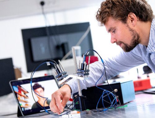
Their method consist in transferring the grow graphene layer from copper roll to plastic foil, where the quality of the process can be determined by using terahertz radiation. A detailed procedure is explained in this (click) short video.

Scheme of a system ensuring continuous quality control of the obtained graphene.
Source: youtube.com/watch?v=C6tBB7zAD_k
Behind the Christmas joke hides an important breakthrough, that enables for constant quality control of the graphene layers. This is the key to achieving stable and reproducible materials for utilising in electronic circuits. Graphene is an excellent conductor of heat and electricity. It is often “sandwiched” between many different layers and materials to be used in electronic and photonic devices. However, controlling the quality of such stacks becomes more complicated and this is where terahertz spectroscopy makes things easier.
Just as X-rays allow us to see inside humans without surgery, terahertz spectroscopy non-invasively penetrates layers in order to provide information about their electrical quality. The newly developed method of terahertz spectroscopy may become the basic research standardizing graphene and increase trust in devices based on its.
More information:
DTU website, Graphene Flagship website and
“Case studies of electrical characterisation of graphene by terahertz time-domain spectroscopy.” P.R. Whelan, B. Zhou, O. Bezencenet, A. Shivayogimath, N. Mishra, Q. Shen, B.S. Jessen, I. Pasternak. D.M.A. Mackenzie, J. Ji, C. Sun, P. Seneor, B. Dlubak, B. Luo, F.W. Østerberg, D. Huang, H. Shi, D. Luo, M. Wang, R.S. Ruoff, B.R.Conran, C. McAleese, C. Huyghebaert, S. Brems, T.J. Booth, I. Napal, W. Strupinski, D.H. Petersen, S. Forti, C. Coletti, A. Jouvray, K.B.K. Teo, A. Centeno, A. Zurutuza, P. Legagneux, P.U. Jepsen, P. Bøggild. 2D Materials (2021), DOI: 10.1088/2053-1583/abdbcb.


